计算机组成原理
概论
高级语言 又称算法语言,面向解决实际问题所用的算法,瞄准处理问题和解题过程的程序
汇编语言 是对计算机机器语言进行符号化处理的结果,再增加一些方便程序设计而实现的扩展功能 在汇编语言中,可以用英文或缩写替代二进制的指令代码,更容易记忆和理解
机器语言 是计算机硬件能直接识别和运行的指令的集合,是二进制码组成的指令 程序最小的执行单元是指令。
翻译程序 将高级语言翻译成机器语言程序的软件
- 编译程序 将用户编写的高级语言程序的全部语句一次全部翻译成机器语言程序
- 解释程序 将源程序的一条语句翻译成对应于机器语言的一条语句,并且立即执行
计算机体系结构 是指那些能够别程序员所见到的计算机系统属性,即概念性的结构和功能特性
计算机组成 是指如何实现计算机体系结构所体现的属性,它包含了许多对程序员来说透明的硬件细节
冯·诺依曼计算机
- 计算机由运算器、存储器、控制器、输出和输入五设备五大部件组成
- 指令和数据以同等地位存放在存储器内,并可以按地址寻访
- 指令和数据均用二进制数表示
- 指令有操作码和地址码组成,操作码用来表示操作的属性,地址码用来表示操作数在存储器中的位置 (在操作数这个字段中可以放操作数本身,也可以放操作地址,还可以放操作地址的计算方法)
- 指令在存储器内按顺序存放,通常指令是顺序执行的,在特定的条件下,可以根据运算结果或设定的条件改变执行顺序
- 机器以运算器为中心,输入输出设备与存储器间的数据传送通过运算器完成(所以有了总线)
CUP Central Processing Unit
ALU Arithmetic Logic Unit 算术逻辑单元,用来完成算术逻辑运算
- ACC Accumulator 累加器
- MQ Multiplier_Quotient Register 乘商寄存器
- X 操作数寄存器
CU Control Unit 控制单元 用来解释存储器中的指令,并发出各种操作命令来执行指令
- PC Program Counter 用来存放当前欲执行的指令地址,和MAR有通路
- IR Instruction Register 用来存放当前指令,从MDR中读取到的指令
- CU Control Unit 用来分析当前指令所需完成的操作,并发出各种微操作命令序列,用以控制所有被控制的对象
一条指令执行包括三个过程:取址、分析、执行
- 取址:命令寄存器读出一条指令
- 分析:对指令分析,指出该完成什么操作,并按照寻址特征指明操作数的地址
- 执行:根据操作数所在的地址以及指令的操作码完成某种操作
MM Main Memory
- MAR Memory Address Register 存储器地址寄存器:用来存放访问单元的地址,位数代表存储单元的个数。
- MDR Memory Data Register 存储器数据寄存器:用来存放从存取体某单元取出的代码或者准备往某存储体存入的代码
现在的CPU中集成了MAR和MDR
机器字长 指CPU一次能够处理数据的位数,通常与寄存器的位数有关
存储容量 = 存储单元个数(MAR) × 存储字长(MDR)
运算速度 用单位时间内执行命令的平均条数来衡量,并用MIPS(Million Instruction Per Second)作为计量单位
CPI Cycle Per Instruction 执行一条指令所需要的的时钟周期(机器主频的导数)
FLOPS Float Point Operation Per Second 每秒浮点运算次数
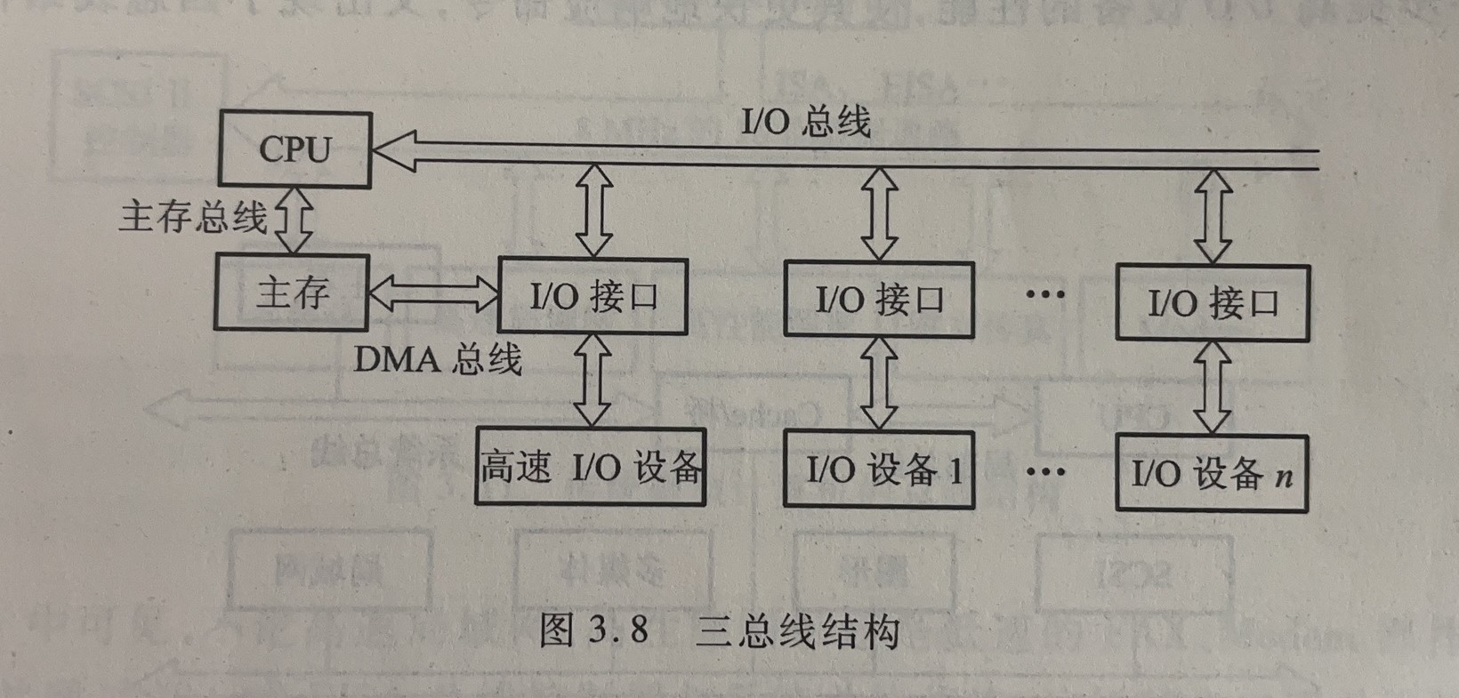
总线
单总线多总线之间的变化:
- 单总线到双总线 将速度较低的I/O设备从从单总线上分离出来
- 双总线到三总线 将I/O总线中高速设备连接到DMA总线上
- 三总线到四总线 将主存总线 分为 局部总线(CPU 和 Cache)和系统总线(MM 和 Cache)
总线通信控制
同步通信
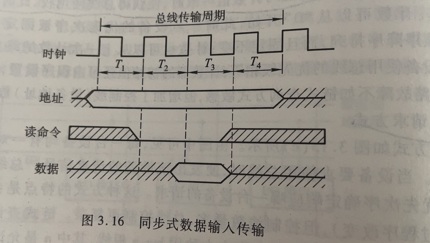 CPU在T1上升沿发出地址信息;在T2上升沿发出读命令;在T3上沿到来之前,将CPU所需要的数据送到数据总线上;在T3始终周期里内将数据线上的信息送到内部寄存器中;在T4的上沿撤销读命令,撤销对数据总线的驱动。
适用于总线长度较短,各部件的存取周期一致的场合
异步通信
异步通信分为不互锁,半互锁,全互锁三种
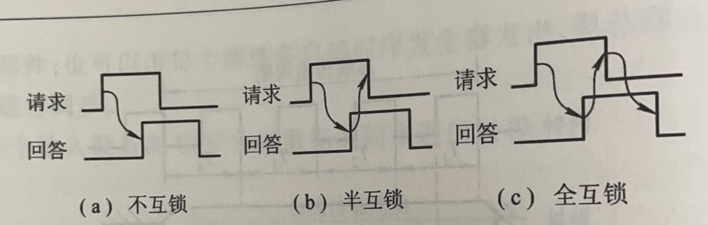 不互锁:主模块发出请求信号后,不必等待从模块的回答信号,而是经过一段时间后,确认从模块已经收到请求信号后,便撤销其请求信号。
半互锁:主模块发出请求信号,必须待接到从模块的回答信号后再撤销其请求信号,有互锁关系;而从模块在接到请求信号发出的回答信号,但不必等待获知主模块的请求信号已经撤销,而是隔一段时间自动撤销回答信号,无互锁关系。
全互锁:主模块发出请求信号,必须待从模块回答后在撤销其请求信号;从模块发出回答信号,必须待获知主模块请求信号已撤销后,在撤销其回答信号。
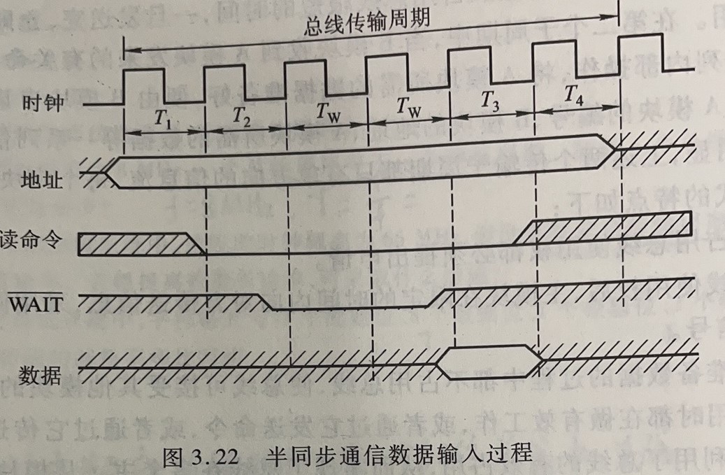 若从模块工作速度慢,在T3时钟周期无法提供数据,则必须在T3到来前通知主模块,给出低电平信号;若主模块在T3周期到来之前检测到了低电平信号,则插入一个时钟周期Tw
分离式通信省略
存储器
RAM(Random Access Memory) 随机存储,存储的时间和存储单位的物理位置无关
- 静态的 SRAM(以触发器原理存储信息)和 动态的 DRAM(以电容充放电原理存储信息 需要每2ms使用刷新放大器刷新 防止信息丢失)
ROM(Read Only Memory) 只能读,不能写入
- MROM 由厂家制作不可再次写入 行列选择线交叉处可以由MOS管 也可以没有
- PROM 由双极电路和熔丝构成 可一次写入不可修改
- EPROM 使用浮动栅MOS电路,给漏端加高电压,浮动栅浮起阻断电路;紫外线照射擦除
- EEPROM 电可擦存储器,Flash Memory
辅存
- 磁盘 光盘 磁带
缓存
- cache
串行存储器 对其读写时,需要按其物理位置的先后顺序寻找地址
存储容量 = 存储单元个数 x 存储字长 (能存储二进制码的总位数)
存储容量 = 存储单元个数 x 存储字长/8 (能存储字节的总位数)
存储速度
- 储周期(连续两次独立的存储操作时间所需的最小间隔时间 MOS 100ns TTL 10ns)
- 存取时间(读或者写时间)
存储器带宽 单位时间内存储的信息量 (T 500ns 16位 带宽为 32M位/秒)
存储器与CPU连接
存储容量的扩展
- 位扩展:增加存储字长
- 字扩展:增加存储器的数量
- 字位同时扩展
地址线的连接:通常将CPU地址线的低位与存储芯的低位相连。CPU的高位用于存储芯扩充,片选线等
数据线的连接:必须对存储芯片扩位,使其数据位数与CPU相等
读写命令线的连接:CPU的读写命令线一般直接和存储芯片的读写端相连,通常高电平位读,低电平位写。
片选线的连接:存储器由许多存储芯片组成,哪一片被选中完全取决于该存储芯片的片选控制端是否接收到来自CPU的片选有效信号;且片选有效信号和访存控制信号有关(若访问I/O,则访存控制信号位高电平,表示不要求存储器工作);CPU中没有与存储芯片连接的高位地址线必须和访存控制信号共同产生存储芯片的片选信号。
存储器的校验
二进制位数为n,需要校验k位,组成n+k位代码满足:2^k >= n + k +1
汉明码偶校验:只需⊕ 1, 3, 5, 7 2, 3, 6, 7 4, 5, 6, 7得到 C1, C2, C3
提高访存速度
单体多字系统:适用于指令和数据在主存内时连续存放的
多体并行系统:采用多体模块组成的存储器。每个模块都有相同的容量和存储速度,各模块都有独立的MAR、MDR、地址译码器、驱动电路和读写电路,他们既能并行工作又能交叉工作。
多体模块由存控器来控制。它由排队器、控制线路、节拍发生器、及标记触发器等组成。
I/O系统
程序查询方式
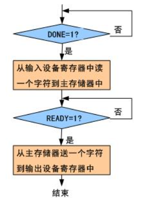
表示从键盘输入一个字符到处理机,再把这个字符输出到显示器上的工作过程。当DONE标志为"1",表示已经从键盘输入一个字符到设备缓冲寄存器,在这个字符被CPU取走后,DONE标志复位。输出设备的标志READY的设置与输入设备正好相反,当READY标志为"1"时,表示设备缓冲寄存器是空的,正准备接收从CPU送来的数据,在设备缓冲寄存器中已经有数据时,READY标志复位,表示输出设备正在把缓冲寄存器中的数据输出到设备上。
中断输入输出方式
当输入设备已经把数据准备就绪,或者输出设备已经空闲时,要主动向CPU发出服务的请求。在CPU方面,每当执行完成一条指令后都要测试有没有外围设备的中断服务请求,如果发现有外围设备的中断服务请求,则要暂时停止当前正在执行的程序,先去为外围设备服务,等服务完成后再继续执行原来的程序。
中断输入输出方式的定义是:当出现来自系统外部,机器内部,甚至处理机本身的任何例外的,或者虽然是事先安排的,但出现在现行程序的什么地方是事先不知道的事件时,CPU暂停执行现行程序,转去处理这些事件,等处理完成后再返回来继续执行原先的程序。
直接存储器访问(DMA)
对于输入设备:
- 从输入介质上读一个字节或字到DMA控制器中的数据缓冲寄存器BD中,如果输入设备是面向字符的,则要把读入的字符装配成字。
- 若一个字还没有装配满,则返回到上面;若校验出错,则发中断申请;若一个字已经装配满,则将BD中的数据送入主存数据寄存器。
- 把主存地址寄存器BA(在DMA控制器中)中的地址送入主存地址寄存器,并且将BA中的地址增值至下一个字地址。
- 把DMA控制器内的数据交换个数计数器BC中的内容减"1"。
- 若BC中的内容为"0",则整个DMA过程全部结束,否则返回到最上面继续进行。
对于输出设备:
- 把主存地址寄存器BA(在DMA控制器中)中的地址送入主存地址寄存器,并启动主存储器,同时将BA中的地址增值至下一个字地址。
- 将主存储器数据寄存器中的数据送入DMA控制器的数据缓冲寄存器BD中。如果输出设备是面向字符的,则要把BD中的数据拆卸字符。
- 把BD中数据逐个字符(对于面向字符的设备)或整个字写到输出介质上。
- 把DMA控制器内的数据交换个数计数器BC中的内容减"1"。
- 若BC中的内容为"0",则整个DMA过程全部结束,否则返回到最上面继续进行。
通道处理机
-
在用户程序中使用访管指令进入管理程序,由CPU通过管理程序组织一个通道程序,并启动通道。
-
通道处理机执行CPU为它组织的通道程序,完成指定的数据输入输出工作。通道被启动后,CPU就可以退出操作系统的管理程序,返回到用户程序中继续执行原来的程序,而通道开始与设备之间的数据传送。当通道处理机执行完通道程序的最后一条通道指令"断开通道指令"时,通道的数据传输工作就全部结束了。
-
通道程序结束后向CPU发中断请求。CPU响应这个中断请求后,第二次进入操作系统,调用管理程序对输入输出中断请求进行处理。 如果是正常结束,管理程序进行必要的登记等工作,如果是故障、错误等异常情况,则进行例外情况处理。然后,CPU返回到用户程序继续执行。
- 字节多路通道
如果连接在通道上的各个设备轮流占用一个很短的时间片(通常小于100微秒)传输一个字节,或者说,不同的设备在它所分得的时间片内与通道在逻辑上建立不同的传输连接,则称为字节交叉方式(Byte-interleave Mode)。如果允许一个设备一次占用通道比较长得时间传输一组数据,或者说,设备与通道的连接可以根据需要维持到一组数据全部传送完成,则称为成组方式(Block Mode)
- 选择通道
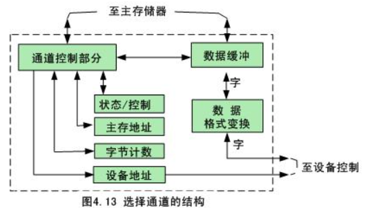
高速外围设备必须设置专门的通道在一段时间内单独为一台外围设备服务,但在不同的时间内仍可以选择不同的设备。一旦选中某一设备,通道就进入"忙"状态,直到该设备的数据传输工作全部结束为止,这就是选择通道(Selector Channel)
- 数组多路通道
从磁盘存储器读出一个文件的过程
第一步是定位,把读写磁头移动到记录该文件的磁道上,这要依靠机械动作来完成,称为定位时间,或找道时间,一般需要十毫秒左右。
第二步是找扇区,等待读写磁头转动到记录该文件的起始扇区位置,称为找扇区时间,或等待时间。等待时间的长短主要与两个因素有关,一是磁盘的转速,二是磁头定位到所需要的磁道时,磁头所处位置与记录该文件的起始扇区位置的相对距离。因此,等待时间的长短是随机的,最长为磁盘转一周所需的时间,最短为零。取平均值,通常称为平均等待时间。目前,高速磁盘的转速已经达到每分钟5000转以上,因此,磁盘存储器的平均等待时间一般小于10毫秒。
第三步是读出数据,目前,高速磁盘存储器的数据传输率已经达到每秒33兆字节以上。因此,读出一个扇区(512个字节)只需要十几微秒时间。
数组多路通道在向一台高速设备发出定位命令后就立即从逻辑上与该设备断开,直到定位完成时再进行连接,发出找扇区命令后再一次断开,直到开始数据传送。因此,数组多路通道的实际工作方式是:通道在为一台高速设备传送数据时,有多台高速设备可以在定位或者在找扇区。
输入输出处理机
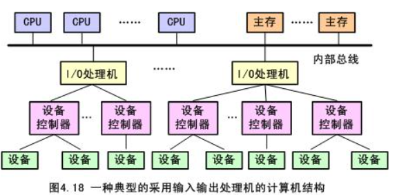 输入输出处理机通常是一台独立的处理机,具有一定的运算功能,可以承担一般的外围处理机的输入输出、控制操作和运算处理等任务。另外,由于输入输出处理机具有自己的存储器,因此,不必通过主存储器就能完成与外围设备的数据交换。
参考文献
[^1] 计算机组成原理 唐朔飞 第二版
[^2] 计算机体系结构 郑纬民,汤志忠 第二版
- 署名:在原有代码和衍生代码中,保留原作者署名及代码来源信息。
- 保留许可证:在原有代码和衍生代码中,保留Apache 2.0协议文件。
- 署名:应在使用本文档的全部或部分内容时候,注明原作者及来源信息。
- 非商业性使用:不得用于商业出版或其他任何带有商业性质的行为。如需商业使用,请联系作者。
- 相同方式共享的条件:在本文档基础上演绎、修改的作品,应当继续以知识共享署名 4.0国际许可协议进行许可。